Context
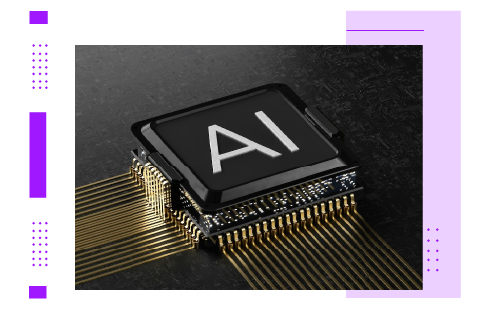
A leading-edge technology firm required the full design and tape out support for an AI- specific System-on-Chip (SoC) featuring a unique AI architecture hardwired into silicon. The chip demanded massive compute density and ultra-high bandwidth memory access for supporting trillion-parameter models.
Eximietas took complete ownership spanning Design Verification (DV), Physical Design (PD), Design for Test (DFT), and Pre-Silicon Firmware Development. The project included setting up the entire design flow and methodologies.
Custom Compute Engine & Memory:
The design incorporated proprietary, custom compute logic optimized for deep learning workloads. This necessitated the integration of a High-Bandwidth Memory (HBM) system for ultra-fast data access, alongside complex central, shared, and private SRAMs for optimized caching. The team managed PD for sub 5nm geometries. Verification Rigor: DV covered all major interfaces (PCIe, Ethernet, HBM, QSPI). Verification included detailed linkup, link training, retraining, TLP testing (Memory, Message, MSI/MSIx), DMA traffic validation, and error handling for HBM. DFT & Validation: Implementation included BISR verification for memory subsystems and complex DFT setup/regression management across multiple blocks.
Flow Setup for Novel Architecture:
Since the design utilized custom compute IP, Eximietas was responsible for establishing the complete physical design flows and methodologies from scratch. Quality of Results (QoR) Optimization: To ensure timing closure and power efficiency in advanced nodes, the team developed specialized tools and a Python-Based Dashboard. This dashboard provided essential insights for efficient data analysis, facilitating continuous optimization of timing and block-level parameters during Physical Design. High-Density Integration: Successful Physical Design and DFT implementation were achieved for this complex, high-pin-count device, leveraging our experience with large CNICs and complex ASICs.
Delivery of a high-performance AI SoC ready for production, showcasing the ability to handle full life-cycle ownership (RTL to GDS2 and ATE prep). Demonstrated expertise in integrating cutting-edge technologies like HBM, PCIe, and custom AI silicon. The project successfully established a robust verification and physical design foundation for high-complexity, advanced node designs (Tape out in 2025).

")
")